THE EXPERT'S VIEW
Micro- and Nanomanufacturing and The Tissue Engineering


This control is what allows one to access new properties that are only manifested on a nanometric scale or to mould the already known ones at will, thus achieving the synthesis of new materials with tailor-made properties and the manufacture of minute, ultrasensitive devices.
The skill in manufacturing structures on a micro- and nanoscale is crucially important, not only in the chips for biomolecular analysis, but in general in the advances in micro- and nanotechnologies and the study of nanosciences. Critical aspects like resolution, dependability, speed and precision are all aspects that need to be taken into account when developing new lithographic processes. So there is a need to develop manufacturing methods that allow the designs and developments of prototypes produced on a laboratory scale to be reproduced as a marketable product. In this respect, when structures with a resolution of above 1 micrometre need to be manufactured, the reference manufacturing technology is conventional Ultraviolet Lithography, in which a thin, photosensitive layer is selectively irradiated by means of 350-450 nanometre light. This technology combines short production times and equipment and maintenance at a lower cost. However, there is no mature technology that offers these features when one is looking for sub-micrometric resolutions, which limits the production on an industrial scale of prototypes built in the ambit of nanotechnology.
Considerable effort has been made when optimizing sub-micrometric lithographic technologies using more energetic sources like extreme ultraviolet lithography, electron lithography, with ion sources or X-ray sources. Nowadays, there are numerous problems when it comes to making these technologies productive; they include: cost, which in some cases exceeds 50 million dollars, or manufacturing time, which is painfully slow for the industry. Only extreme ultraviolet lithography, a technology used by the semiconductor industry to incorporate integrated circuits onto a chip, offers an alternative. However, its cost in terms of investment and annual maintenance is only within reach of very high annual output rates, which is the case of the semiconductor industry. This fact, added to the emergence of applications not connected with microelectronics, many of which are in the field of biotechnology and biomedical applications, has prompted many researchers to invest resources in the quest for alternatives that combine high resolution at an affordable cost. Some important technologies developed in recent years are: microcontact printing, lithography based on atomic force microscopy, nanoimprint lithography or dip-pen lithography, in which a cantilever is used to transfer molecules to the substrate by capillary means. Among all these technologies, nanoimprint lithography is by far the most mature and is being used to manufacture organic lasers, organic light emitting diodes (OLEDS), substrates for tissue engineering and biochips for biomoleculessensing. This technology is being used for production purposes in the manufacture of photonic elements for the optical industry and will shortly be substituting ultraviolet photolithography in the production of data storage units and displays.
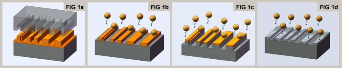
The principle behind Nanoimprint Lithography (NIL) is very simple. A pattern, normally made of silicon, is transferred to a thin polymer layer that coats the substrate –normally made of glass or silicon– under controlled imprint and temperature conditions (Figure 1a). This imprinting process produces a very thin residual polymer layer, which is removed by means of oxygen anisotropic plasma etching until the substrate is reached (Figure 1b). After that, it is possible to carry out the transfer of pattern to the substrate through anisotropic etching in vacuum, using specific gases for this purpose and with the polymer acting as a mask (Figure 1c), or else a thin metal layer can be evaporated on the substrate with the subsequent removing of the polymer in organic solvent (Figure 1d). The process allows the copying of substrates using the stamp within less than 15 minutes to be made, and achieves a minimum resolution mainly determined by the pattern on the stamp, which can be less than 10nm. This is the reason why this technology has attracted the full attention of the industry and R+D centres only a few years after it was proposed at the University of Princeton by the S.Y. Chou group in 1995.
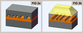
Nanoimprint lithography has two distinct processes. Thermal nanoimprint (Thermal NIL) uses a rigid imprint stamp –usually of silicon– and pressure is applied –of the order of 10-25 bar– to a thin layer of thermoplastic material above its vitreous transition temperature, which allows the material to flow and fill the cavities in the pattern (Figure 2a). After that, the pattern-substrate unit is cooled down and removed from the mould at a temperature lower than that of vitreous transition. Nanoimprinting based on ultraviolet light (UV-NIL) uses rigid, transparent patterns –quartz– or soft ones –silicone– to transfer the structure of the mould to the polymer by applying slight pressure –of the order of 1 bar– and polymer curing is carried out by means of ultraviolet light (Figure 2b). Over the last three years commercial systems similar to steppers used in photolithography by the micro-electronics industry have been developed, thus enabling the imprinting of large areas using a reduced area pattern on the stamp.
The Micro- and Nanomanufacturing Unit has developed this technology and, now that the manufacturing processes have been optimized, is applying it in the field of healthcare to develop diagnostics systems based on DNA stretching in nanofluidic devices, organic semiconductor lasers, or surface modification by means of morphological patterns and biochemical patterns on polysaccharide-based natural polymers.
Tissue Engineering
Research on kits that allow an optimum differentiation of stem cells into different cell lines to be made (bone, cartilage, skin cells, etc.) without resorting to high concentrations of growth factors, is a field of research that has been very active in recent years. The aim being pursued is not only in vitro differentiation and the inserting of the material into the zone to be regenerated (ranging from skin to vital organs) but also the carrying out of the graft and in vivo differentiation. So work has been done to obtain extracellular matrices, in two as well as in three dimensions, in different materials representing the surface on which the cell moves. So the way in which the topography of the material controlled on the micrometre and nanometre scale plays a crucial role in cell morphology (alignment, stretching, dispersion) and the considerable effect it has on cell differentiation and proliferation has been studied; the latter being the reason why an important area of research is focusing on preventing the proliferation and spread of tumour cells.
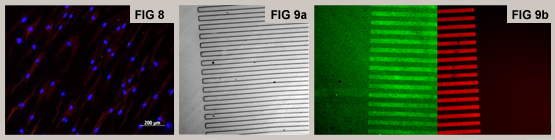
The Micro- and Nanomanufacturing Unit initially studied how the topography influenced the morphology and differentiation of mesenchymal stem cells in bone cells (osteoblasts), by analysing parameters like alignment, stretching, area occupied by the cell and production of the alkaline phosphatase enzyme in this differentiation (Figure 8). This study was carried out on biocompatible, biodegradable synthetic materials like polycaprolactone.
Today, work is being conducted on polysaccharide-based natural materials, which are obtained through natural means and waste, like chondroitin sulphate and various by-products of hyaluronic acid. These materials, which are much more complex to process than synthetic ones, have been studied and optimized to allow their micro- and nanostructuring to be made by means of UV-NIL (Figure 9a). The combination of micro-contact printing with polyelectrolytes that resist the absorption of proteins (PLL-g-PEG molecules) has made it possible to immobilise protein patterns on these materials, by developing protein patterns like streptavidin, albumin or fibronectin (Figure 9b), providing anchorage points to the cellular membrane, and therefore, influencing their movement and differentiation. Today, work is being done to produce a kit that will allow an optimum differentiation of mesenchymal stem cells in bone cells.